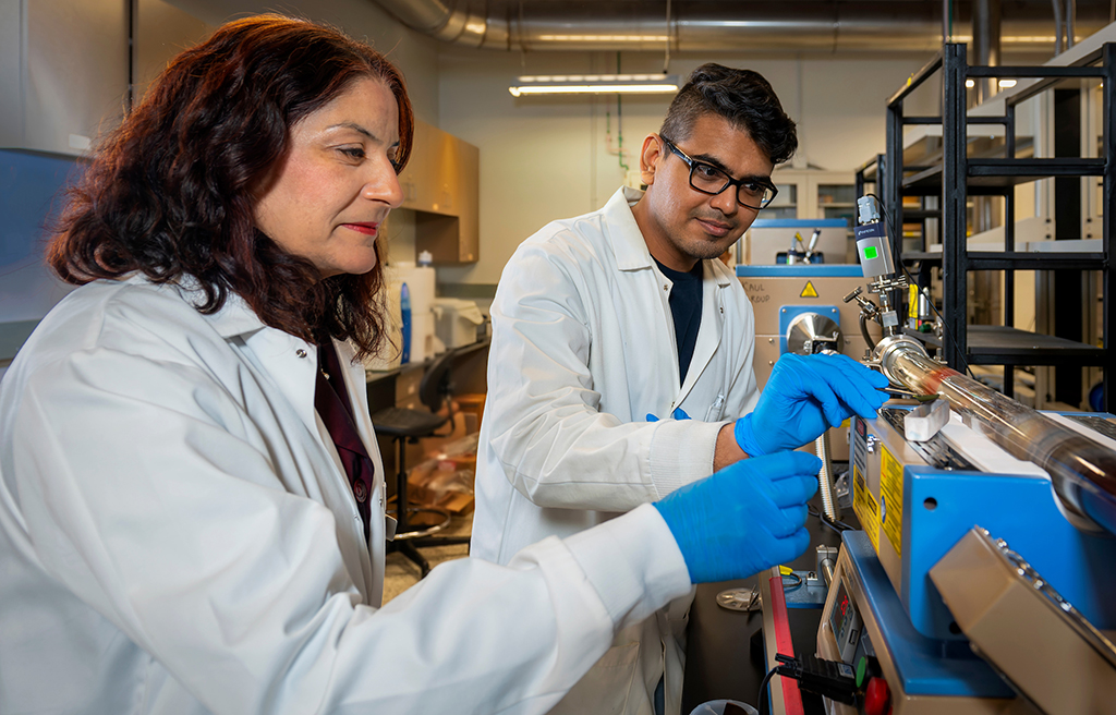
To help address national security concerns about high-performance computing related to information science, Anupama Kaul, professor of materials science and engineering and electrical engineering, is studying nanomaterials such as tungsten diselenide and other semiconducting van der Waals solids that are being considered for electronics as alternatives to silicon. She received a $450,000 grant from the Air Force Office of Scientific Research to offer a number of exploratory solutions for silicon’s inefficiencies.
“The trillion-dollar silicon electronics industry is facing dire challenges at this time from energy inefficiency within the switching states of the transistor. A lot of heat is dissipated in our devices such as laptops or iPhones,” says Kaul, who directs the Nanoscale Materials and Devices Lab and the PACCAR Technology Institute in UNT’s College of Engineering. “And this dissipation is driven by silicon’s inefficiencies at nanoscale dimensions, where transistor scaling is reaching a brick wall in terms of Moore’s Law.”
Moore’s Law refers to Gordon Moore’s 1965 prediction that the number of components on an integrated circuit would double every two years. Industry experts believe that ability to put more components on a silicon chip is nearing its end. Kaul is among researchers working on advanced materials that can help address bottlenecks we face with silicon. Kaul’s research is on two-dimensional layered materials (2DLMs), which can be built up in layered sheets on a chip — on top of silicon or other substrates.
“There’s a lot of energy wasted even in the off-state with silicon transistors, particularly at nanoscale dimensions,” Kaul says. “The 2DLMs could enable higher performance computation devices that could make portable devices like cell phones more energy efficient. The key benefits these materials have over silicon or other conventional 3D semiconductors is their near-perfect, more-pristine atomic interfaces. Since these interfaces have fewer defects or unsatisfied atomic bonds, it allows electrons to carry electricity efficiently without losing energy through collisions at poorly defined atomic interfaces with a lot of obstacles.”
Through her research, Kaul will be examining ways in which to grow these materials over larger areas using high-temperature vapor-based growth techniques. She also will devise novel ways in which to measure their crystalline quality and integration into nanoelectronic, photonic and quantum-devices, including through stacking heterostructures of different layers.
“There are some national initiatives that are ongoing, which tungsten diselenide caters to — for example the National Quantum Initiative, which is a very large effort involving multimillion dollar efforts around the country for quantum computing,” Kaul says.
Quantum computing is envisioned as a way to combat the limitations of Moore’s Law by enabling calculations that go beyond just binary calculations — 1s or 0s.
“At the heart of silicon transistors, all the logic decisions are based on this binary model — yes or no, on or off. That intrinsic single device is what’s controlling billions of transistors on a chip,” Kaul explains. “Quantum is not like that. We don’t have this binary case. We can have multiple states. It gives us many, many options and the ability to do parallel logic computations.”
Kaul’s research is in the early stage and while not directly related to funding from the National Quantum Initiative Act, which passed in 2018 to ensure the continued leadership of the U.S. in quantum information science by accelerating quantum research and development, her lab is studying basic science that will support the initiative.
“There’s an area called quantum photonics — instead of using electrons in a transistor to represent on and off, you could actually communicate with photons. Photons have no mass, and they travel at the speed of light,” Kaul says. “In quantum computing, single-photon emission sources are needed using novel materials. Some of the early work that’s been done with tungsten diselenide suggests that it’s possible to have single photon emission when the system is cooled, and there is potential to make all of this on a chip.”
“Quantum computing is under discussion at very high levels and impacts our national security,” Kaul says. “It’s also economic. There’s a parallel discussion happening in the context of the semiconductor manufacturing to bring it back here in the U.S. so we’re not so dependent on semiconductor manufacturing facilities abroad.”